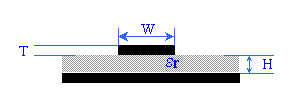
 Microstrip Trace |
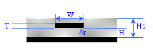 Embedded Microstrip Trace |
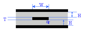 Stripline Trace |
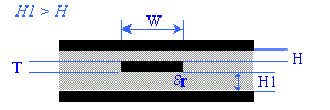 Asymmetric Stripline Trace |
| W: | trace width | |
| T: | trace thickness | |
| H (/H1) | height of trace or dielectric above return plane | |
| C: | distance between the differential stripline pair | |
| er: | relative permittivity of the dielectric |
Electrical Parameter Definitions
| Zo: | characteristic impedance | |
| Zc: | effective characteristic impedance including the capacitance of distributed loads | |
| Tpd: | propagation delay | |
| Lo: | inductance per unit length | |
| Co: | capacitance per unit length |
Acknowledgements:
The source for formulas used in this calculator (except where otherwise noted) is:
IPC-D-317A, Design Guidelines for Electronic Packaging Utilizing High-Speed
Techniques, Jan 1995; Section 5, pp. 13 - 36.
THESE FORMULAS ARE APPROXIMATIONS!
They should not be used when a high degree
of accuracy is required.
The transmission line calculator concept was developed by Douglas Brooks and is described in his paper: PCB Impedance Control: Formulas and Resources, Printed Circuit Design Magazine, March 1998. A copy of his paper and a similar transmission line calculator that runs on a PC can be obtained from UltraCAD Design, Inc.